New Horizons in Micro-Optical Assembly Fabrication
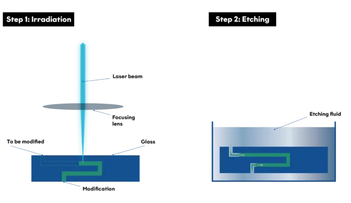
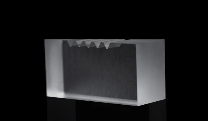
The rapid evolution of optical technologies in telecommunications, quantum computing, medical devices, and semiconductor manufacturing is fundamentally changing the requirements for micro-optical assemblies and their fabrication. Selective Laser-Induced Etching (SLE) can provide a solution, as a two-step process (Figure 1) that enables the fabrication of complex 3D microstructures in transparent materials such as fused silica, borosilicate glass, and to some degree even sapphire.
Step 1: Laser modification
A focused femtosecond laser beam is scanned within the bulk of the substrate, locally modifying the material’s structure at precise 3D coordinates. The laser parameters (pulse energy, repetition rate, scanning speed) are carefully controlled to induce changes in the material’s etch rate without causing cracks or significant thermal damage. The modified zones can be as small as a few micrometers in diameter, and the process can be repeated at multiple depths to create intricate internal geometries.
Step 2: Chemical etching
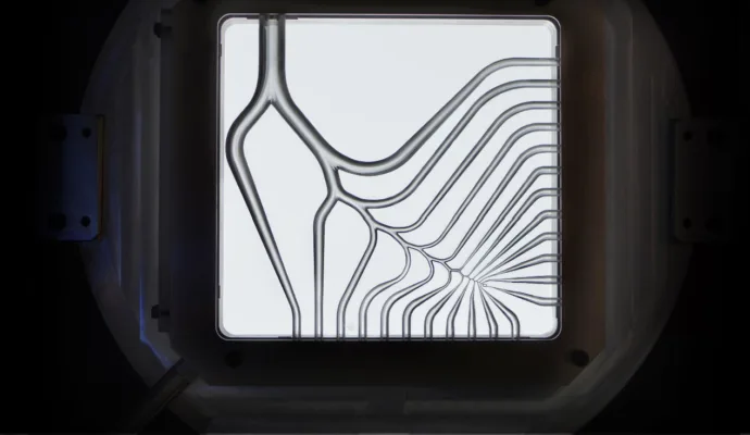
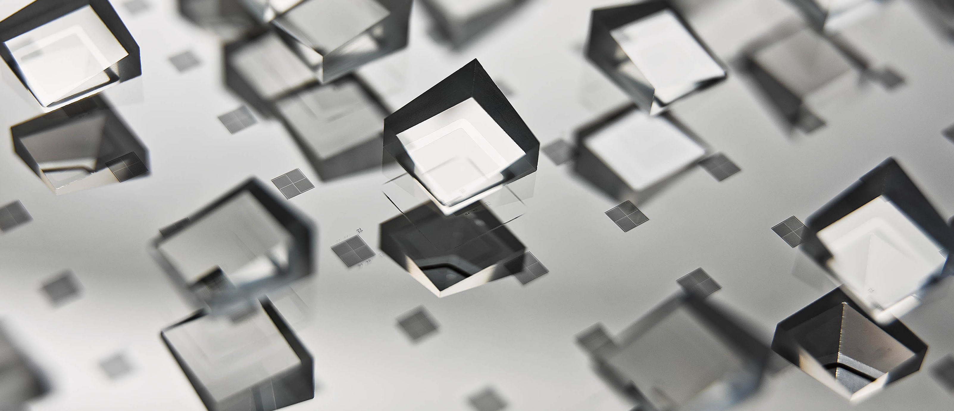
The laser-modified substrate is then immersed in a suitable chemical etchant (for example, KOH or HF solution). The modified regions dissolve much faster than the unmodified material, allowing selective removal of the desired structures. The result is a monolithic component with complex 3D features, such as microchannels, glue pockets, alignment structures or even flexures, all integrated within a single piece of material.
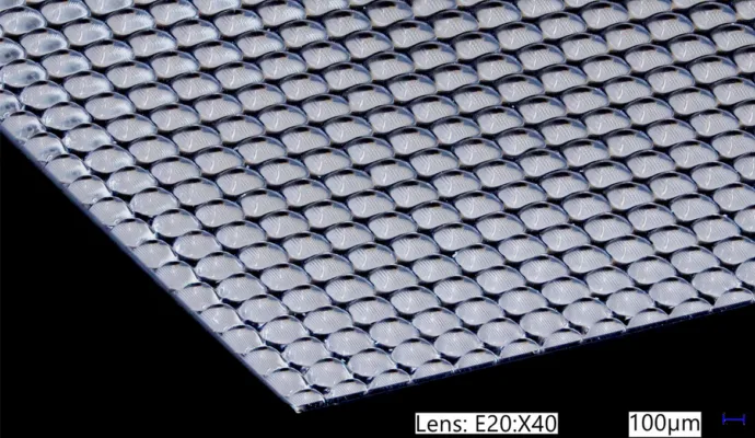
While SLE provides excellent control over geometry and feature size, the resulting surface roughness is typically in the range of 100-500 nm Ra. This is sufficient for most microfluidic and mechanical applications, depending on process parameters and etchant chemistry. Achieving surface roughness around 10 nm Ra is not feasible with SLE alone, but possible with CO2 laser polishing, which is also done in-house. In this process, the laser energy melts the surface allowing surface tension to smooth out micro-scale irregularities before re-solidification.
Overcoming industry limitations
The combination of SLE with optical assembly and CO₂ laser polishing introduces new technical capabilities in the fields of photonics, semiconductor/electronics fabrication, and medical technology. Below, several use cases that reflect the capabilities of this technique are detailed.

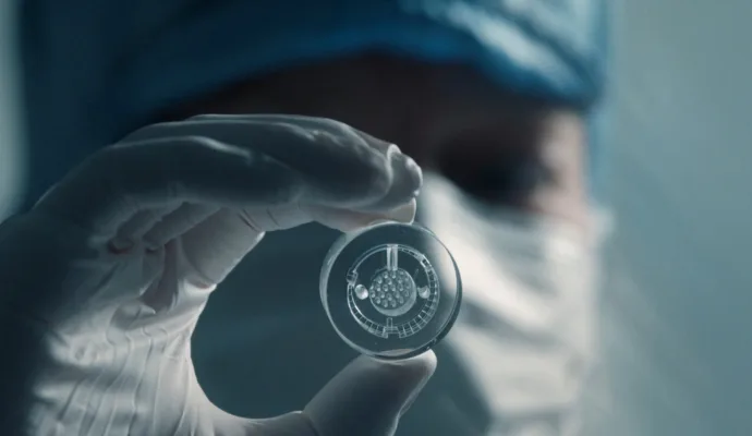
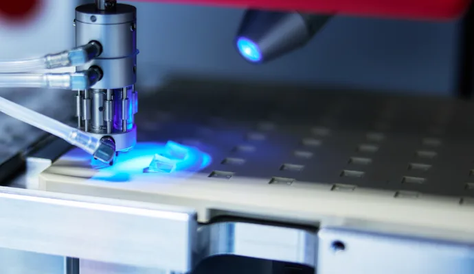
At LouwersHanique, SLE-fabricated components are integrated into complete assemblies using state-of-the-art pick & place automation in ISO 7 cleanrooms. The modular pick & place system with submicron repeatability handles delicate micro-optical parts, positioning them with six degrees of freedom and with far greater accuracy and consistency than manual methods can achieve. Submicron positioning of droplets with volumes down to 2 nanolitre combined with active alignment techniques and force-controlled placement of components, ensures optimal adhesion without compromising the optical path. Due to the modularity of the system, it is highly customisable to specific product needs.
Hybrid integration, combining SLE-fabricated glass parts with metallic housings, semiconductor chips, or polymer elements, is also possible, enabling the creation of multifunctional photonic modules. The result is a scalable, reliable process suitable for both prototyping and series production, supporting the stringent requirements of telecom, quantum, semiconductor/electronics and medical markets.
Martin Hermans is a Senior Engineer in the R&D department at LouwersHanique. He focuses on optimizing existing laser technologies and exploring new laser technologies and applications to expand the company’s capabilities in high-end machining of technical glass and ceramic materials.